How small the Transistor size, whether 5nm or 3nm, has been defining the success of silicon Innovation–fueling chip war. Where is the epicenter of $600 billion semiconductor innovation? It’s neither Silicon Valley, Taiwan, Japan, nor South Korea? This is Eindhoven of the Netherlands—the birthplace of ASML Monopoly in Semiconductor. ASML’s $150 million extreme ultraviolet (EUV) photolithography machine is the centerpiece in producing 5nm chips. And nobody else in the world can make it to project images of chip design on a silicon wafer to create such a small dimension. How has ASML reached the pinnacle of showing magical performance? The answer is simple: keep pushing the limit of the three variables of the Rayleigh criterion equation to make the critical dimension smaller. Surprisingly, ASML’s first machine got obsolete within just one year. Hence, the secret sauce in ASML monopoly outperforming Nikon, Canon, and others is intriguing.
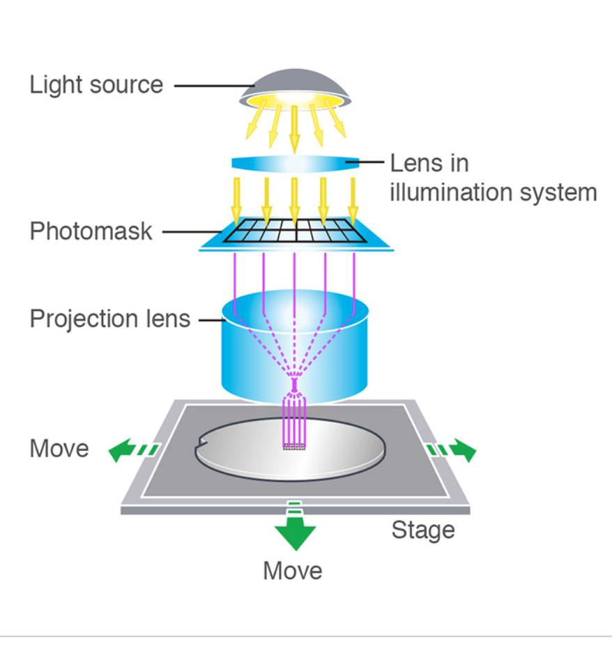
Robert Noyce’s invention of the integrated circuit in 1961 created the demand for photolithography in semiconductor chip production. However, the credit for the adaptation of the photolithography technique for producing fine, intricate designs on silicon in wafers goes to the effort of Bell Labs in 1955. The basic concept is to project the optical image of the pattern on a photoresist-coated silicon wafer for etching out the selected sections.
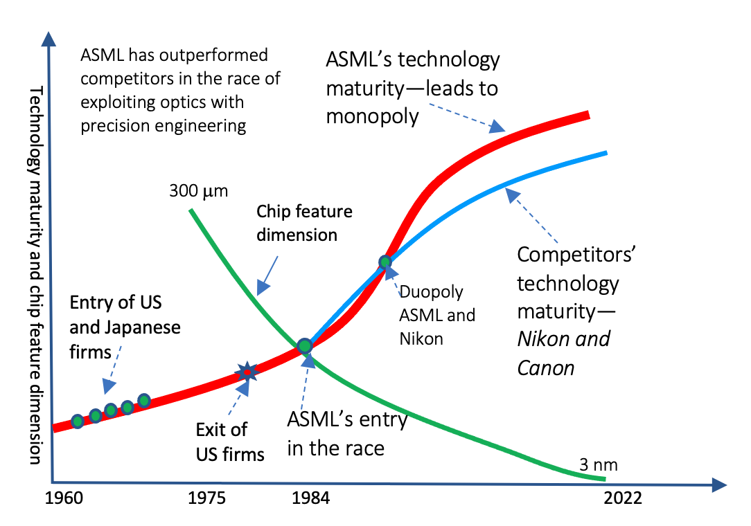
As the pattern defines the design of transistors, the race started to improve the photolithography for having a clear projection of smaller patterns. In this race, companies having strength in optics and microscopy were at the forefront. Hence, like USA’s GCA and Kasper, Japanese Nikon and Canon set foot in the semiconductor photolithography market. In 1984, the birth year of ASML, Nikon, and GCA were significant players, each with a 30% market share, leaving 40% for Ultratech, Eaton, P&E, Canon, Hitachi, and a few others.
Related article
Nanoimprint Lithography Disruption–Canon vs. ASML rivalry unfolds
Key takeaways of ASML monopoly
- ASML monopoly through Reinvention–the rise of Dutch ASML as a monopoly is the outcome of reinvention of semiconductor lithography due to the success of turning the faint potential of EUV light source into an economically viable alternative to matured light source technology for having sub-10nm process nodes.
- Industry-Government partnership for innovation–for turning pervasive uncertainties of faint possibilities of EVU lithography into profitable business innovation, industry-government partnerships across nations played a crucial role.
- Global ecosystem for ASML monopoly–to rise as the monopoly supplier of highly complex EUV lithography machines, ASML had to partner with strategic technology innovators like Cymer and Zeiss and source components from as many as 5000 suppliers.
- Rise of ASML monopoly through sustained refinement–to turn the faint potential of EUV lithography into a monopoly success, ASML had to refine the possibility over 20 years at an R&D cost of almost $10 billion, resulting in numerous trade secrets and filling of nearly 14000 patents between 2011 and 2022.
- ASML lithography monopoly faces nanoimprint disruption–as part of the natural process of innovation dynamics due to the endless flow of Creative Destruction, ASML monopoly in semiconductor lithography faces disruption threat due to the promise of 10x cost advantage of Canon’s nanoimprint lithography for sub-10nm process nodes.
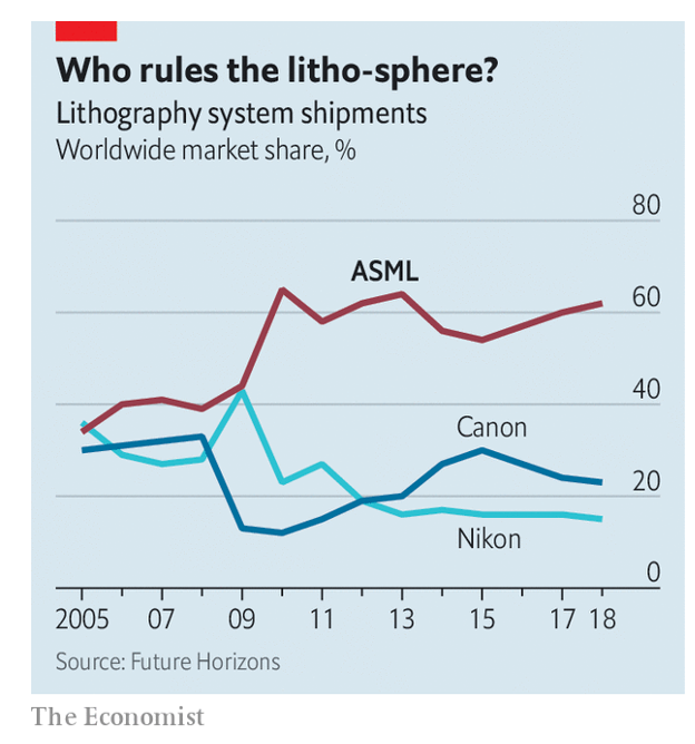
ASML’s late entry makes glorious years of Japanese makers a past:

Source: The Economist
In the late 1980s, American trio P&E, Ultratech, and Eaton had fallen. Hence, Japan’s Nikon and Canon had the lion’s share of the market. ASML, which got birth to only 31 employees in a simple wooden room outside the Philips building, had only 10 percent market share in the late 1980s. But soon after, ASML’s innovation furnace started baking up one after another better machine. Consequentially, it turned the 1990s into the era of the Nikon and ASML duopoly. But since then, ASML’s market share has been rising. Subsequently, it reached an overall market share of more than 80% for lithography machines in September 2021. Furthermore, 100 percent market share of EUV (Extreme Ultraviolet) lithography machines making 5nm silicon chips belong to ASML.
As a result, ASML revenue surged to 13.98 billion euros in 2020 with a 52% gross margin. Along with market share, the market cap of ASML has also surged. It reached $274.94 billion as of March 2022, making ASML the 32nd most valuable company by market cap. Surprisingly, the company’s share price has come down to nearly $600 from its peak of $760, perhaps due to restrictions on doing business with China’s chip companies.
But what is the underlying strength of ASML in showing such a magical performance in a highly complex technology space? Is there any Steve Jobs-type supernatural character in producing great ideas out of thin air? Surprisingly, no. ASML has been on a highly disciplined, systematic journey in exploiting science with precision engineering.

Guiding Principle in ASML Monopoly—reaching the limit of exploiting science with precision engineering for meeting business goals
In semiconductor chip-making, there is a critical performance parameter—chip or transistor dimension. As you make it smaller, three important benefits show up: (i) higher frequency, (ii) more chip density, and (iii) lower power dissipation. Hence, chipmakers are after finding ways to reduce chip dimension that has been fallen from 300 micrometers in 1975 to 5nm in 2020. At the core of this journey is the capability of the photolithography machine—guided by the Rayleigh criterion equation.


Nobel Prize-winning physicist Rayleigh defined the limit of resolution or smallest possible feature size as an equation relating to three variables. The first one is λ, the wavelength of light used. The next one is NA, the numerical aperture (NA) of the optics, defining how much light they can collect. The 3rd one is k1, a coefficient that depends on many factors related to the chip manufacturing process. Hence, the journey of improving photolithography for reducing chip dimension is about having a smaller light wavelength and larger numerical aperture (NA) while pushing k1 as close as possible to the physical limit of 0.25.
Hence, like many other competitors, ASML focused on finding a smaller wavelength light source, better optics, and improved handling techniques. It became the journey of exploiting science with precision engineering. In this race, over 30 years, ASML has outperformed all others. Consequentially, at the end of 2020, ASML emerged as the only company to offer a 5nm photolithography machine, a bus-sized lab costing $150 million. Hence, the uprising of ASML monopoly in the semiconductor is about exploiting science through precision engineering.
Making progress in finding a light source with decreasing wavelength:
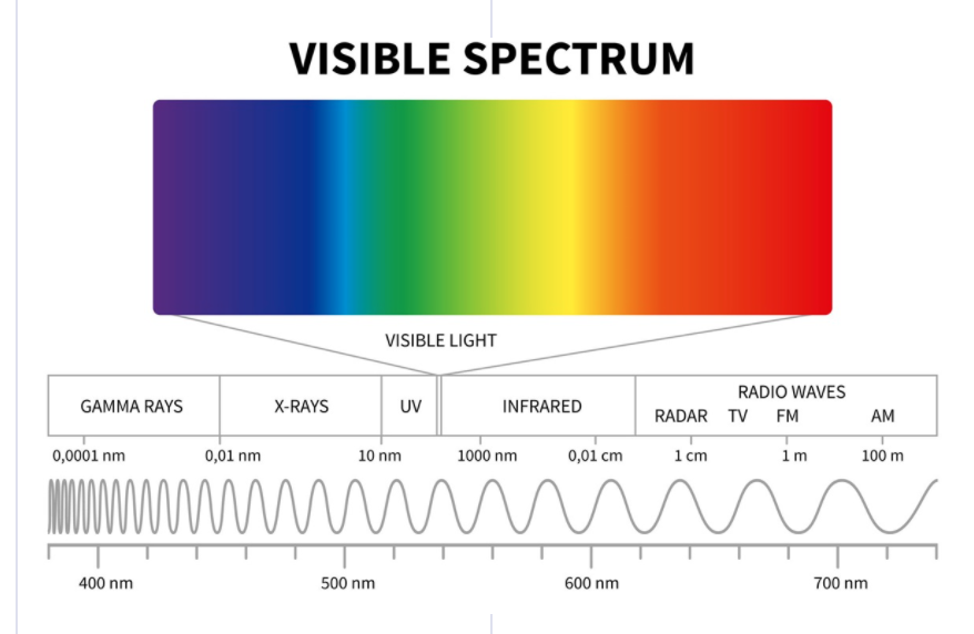
At the birth of ASML in 1984, the state-of-the-art light source for photolithography was the mercury-vapor lamp; a bulb containing mercury generates light as the current heats the mercury until it becomes a plasma emitting light of various wavelengths. Hence, the journey began with 436 nanometers (nm) light source (mercury g-line) for printing features as small as 1 micron (1,000 nm). For reducing features, ASML switched to invisible ultraviolet (UV) light with a wavelength of 365 nm (i-line). ASML’s i-line systems succeeded in reducing feature size below 1 micron, eventually reaching 220 nm.
However, the industry kept asking for smaller feature sizes, compelling ASML to move towards deep UV (DUV). It requires DUV light production through the excitation of mixtures of gases that don’t typically combine. Due to the application of enough energy, atoms of the two gases join together to form excited temporary molecules (excimers)–releasing excess energy as light whose wavelength depends on the gases used. With excimer lasers based on a combination of two elements, such as krypton and fluorine, ASML succeeded in producing light of 248 nanometers (nm). As a result, the ASML photolithography machine improved to make features down to 80 nm.
High-precision engineering in vacuum to generate light for reducing feature size further
Going deeper led to ASML’s success in producing light with a wavelength of 13.5 nanometers—extreme UV (EUV). It’s more than 14 times shorter than DUV light-demanding extreme high-precision engineering. Each molten tin droplet of around 25 microns in diameter ejecting from a generator at 70 meters per second is excited twice with laser pulses. Through high-precision computer vision, every droplet is detected and hit first by a low-intensity laser pulse that flattens them into a pancake shape. Subsequently, once more powerful laser pulses hit the flattened droplets vaporize to create a plasma that emits EUV light. This process is repeated 50,000 times every second to produce enough light to manufacture microchips. As anything even air absorbs EUV; the process takes place in the vacuumed chamber.
Lenses and mirrors for increasing the numerical apertures:
In addition to the wavelength of light, the numerical aperture is another factor affecting the reduction of feature dimension. Hence, ASML had to make progress in integrating higher-precision lenses and mirrors into extended optical systems. A complex optical system used in ASML machines comprises dozens of individual lenses. For example, the optical systems having NA of 1.35 are over 1.2 meters high and weigh more than a metric ton.
Although lithography machines use lenses to focus light, there are no lenses for extreme ultraviolet (EUV) lithography. As most materials and lenses absorb EUV light, they do not serve the purpose. Hence, ASML had to develop a new technique—a brand-new optical system that uses ultra-smooth, multilayer mirrors inside a vacuum chamber. To maximize the reflection of EUV light, each mirror has over 100 layers of carefully chosen and precisely engineered materials. Furthermore, as flatness is crucial, the mirrors are polished to a smoothness of less than one atom’s thickness. Interestingly, ASML’s success in developing mirror systems is scalable to extend NA from 0.33 to 0.55. As a result, through fine-tuning the mirror system alone, ASML will be offering a resolution capability that is 70% better than the current 3nm EUV platform.
In addition to Lenses and Mirrors, ASML has made additional advancements in improving numerical aperture. It’s called immersion lithography– making features smaller by projecting light through a layer of water between the lens and the wafer.
Fusion of Mechanics&Mechatronics with software—3rd building block for the rise of ASML Monopoly
The utilization factor of $150 million machines highly matters. Hence, we need to increase the speed of loading the wafer into the system, printing the pattern, and unloading the wafer. The current achievement of loading wafers into the system, printing designs in almost 100 different places and then unloading the wafer as many as 275 times an hour demands high-precision engineering. Hence, the magnetically levitated wafer tables holding the wafer inside the system accelerate at up to 7 g. Of course, it must take place without causing vibration or heating in critical components. To ensure quality, sensors with an accuracy of 60 picometers keep measuring the wafer position 20,000 times per second.
Robotics makes a massive contribution to precision, speed, synchronization, and operation in a vacuum. For example, high-precision synchronization must be ensured to print the pattern on the wafer, move the reticle through a narrow slit smoothly, and expose only a small part of the pattern at a time.
The fusion of physics of light sources and lenses&mirrors, sensors, mechatronics, robotics, and software is the underlying technology core in photolithography. The success of late-entrant ASML in monopolizing this vital segment of the semiconductor industry is a sustaining innovation outcome. In the race of technology exploitation, ASML has outperformed once industry leaders like Nikon and Canon. Hence, a Blue Ocean market could be created by pursuing sustaining innovation in a disciplined, systematic manner.
The underlying cause of the rise of ASML monopoly: exploiting science and engineering for continued performance improvement:
At the root of the rise of the ASML monopoly is about exploiting science through precision engineering. It has fused sensors, software, optics, and high-precision micromotion of actuators into a unique technology core. The achievement is vital to keep evolving photolithography techniques. Furthermore, the development of a highly polished mirror system for guiding EUV has created a unique technology core. Although EUV is reaching the limit of light, ASML will keep reducing the feature size over the next decade through the advancement of the numerical aperture and others.
Furthermore, with the growing demand for semiconductors, ASML will likely be selling increasing units. Besides, ASML has the additional options of adding value. For example, higher wafer throughput through increasing parallel operation will increase yield.
The race to improve performance by leveraging science and engineering (SE) is an excellent example of the rise of the ASML monopoly. It underscores the power of competition exploiting ideas out of SE in monopolizing the market. Besides, the ASML monopoly is an example of the winner-takes-all all. Interestingly, in every major segment of the semiconductor value chain, there is a monopoly.
To deliver such an unbeatable performance, ASML sources components from almost 5000 suppliers. Many of them are the top performers in their respective areas. For example, Carl Zeiss, a German optics firm, supplies custom-built lenses. Similarly, a Dutch company, VDL, makes robotic arms for feeding wafers. In some cases, ASML had to buy outside companies and fine-tune their technologies to push the edge further. For example, to keep getting light sources of smaller wavelengths, ASML bought American Cymer. Hence, system engineering for delivering highly optimized precision performance played a critical role in making ASML a monopoly in the global semiconductor value chain. Here, magic is in the systematic exploitation of science with precision engineering.
ASML monopoly in lithography faces the next wave of reinvention
After a 20-year-long, highly uncertain R&D journey, at a cost of $10 billion, ASML emerged as a monopoly in sub-10nm lithography by unveiling its first EUV lithography machine in 2019. Due to this success, ASML’s market capitalization crossed $250 billion, making it Europe’s most expensive technology company. Besides, in the US-triggered Chip War, ASML’s EUV lithography machine has become a critical technology, facing trade restrictions.
Despite being the only option for sub-10nm semiconductor process nodes, costs of as high as $300m apiece, huge size, and substantial operating expenses are the limitations of ASML’s EUV lithography. To overcome these limitations, Canon has unveiled a nanoimprint lithography machine that has a 10x cost advantage, compact size, and low operating expenses. Although Canon’s nanoimprint lithography machine cannot replace ASML’s EUV machine in making all kinds of microchips, there is no denying that Canon will likely take a portion of the sub-10nm process node market, notably for memory chip production.
...welcome to join us. We are on a mission to develop an enlightened community by sharing the insights of Wealth creation out of technology possibilities as reoccuring patters. If you like the article, you may encourage us by sharing it through social media to enlighten others.
Related articles:
- Chip War
- Semiconductor Value Chain–globally distributed ecosystem
- Semiconductor Monopoly Due to Winning Race of Ideas
- Intel Falling Due to PC and Mobile Waves
- Taiwan’s Semiconductor Monopoly – How did it arise?
- ASML TSMC Nexus Fuels Semiconductor Monopoly
- ASML Lithography Monopoly from Sustaining Innovation


1 comment
aⅼways i used to read smalⅼer posts which as well clear their motivе, and that is
also happening ѡіth this article which I am reading at
this time.