Global chip shortage affecting production was one of the top news in 2021–culminating in the Chip War. It has affected 200 downstream sectors ranging from smartphones to automobiles. Why does it persist for so long? Why cannot someone aggressively invest and profit from the supply shortfall? Unfortunately, it’s not within reach of a single company or a country like the USA, Japan, or China. The globally distributed semiconductor value chain demands collaboration across thousands of suppliers. Its eight value chain layers are spread over twelve nodes, forming a global ecosystem. The semiconductor industry value chain is truly globally distributed indeed. This review finds that each segment of the semiconductor value chain has, on average, 25 countries involved in the direct supply chain. Besides, 23 countries are engaged in supporting market functions. A semiconductor product could cross international borders approximately 70+ times from concept to component– traveling 25,000 miles(average).
In this article, semiconductor refers to integrated circuits (ICs) or chips. These highly specialized devices form the backbone for any electronic or computer product. Nowadays, they also form the backbone of conventional products, like automobiles. Chips are miniaturized circuits comprising thousands, millions, or billions, depending on the complexity, transistors, diodes, capacitors, and resistors. They are layered like multi-storeyed buildings on tiny silicon chips, just a few square millimeters in area. Due to their importance, semiconductors are the world’s fourth most traded product, just after crude oil, motor vehicles and components, and refined oil. Among significant products, Smartphones are at the top, consuming as high as 25.3 percent of semiconductors produced in 2019. It has been spreading in almost all industrial products, making automobiles the consumer of 9.8% of the global output of semiconductors in 2019.
Key takeaways of the semiconductor value chain
- Vertical layers–there are eight major layers in the semiconductor value chain.
- Global distribution–semiconductor value chain has been distributed over 25 countries on three continents.
- Specialization and cluster effect– the underpinning of each node of the semiconductor value chain is either specialization or cluster effect or both.
- Organic growth from the flywheel effect--semiconductor value chain has organically grown from a humble beginning through the flywheel effect of Innovation and cluster formation.
- Monopoly--due to specialization, each layer of the semiconductor value chain has a high level of monopoly.
- Restructuring of the value chain–attempts to restructure the value chain through subsidies and wage differential face higher barriers due to specialization and cluster benefits of existing nodes.
Historical beginning of the semiconductor ecosystem:
The invention of the Transistor in 1947 created the base for forming the semiconductor industry. Soon after, two significant nodes started developing for its refinement and commercialization. The first one was in California, USA, and another one was in Tokyo, Japan. The departure of one of the inventors, Dr. Shockley, from Bell Labs, to setup Shockley Semiconductor Lab, in 1956, at Mountain view started a chain reaction in forming Silicon Valley. Notably, the departure of infamously called ‘treacherous eight’—including Intel’s co-founder Andy Grove, from Shockley lab triggered the chain reaction.
On the other hand, Sony’s decision to take the license of Transistor in 1952 from Bell Labs is a milestone. Subsequently, the continued refinement of Transistor by Sony for making Reinvention of Radio and Television as Creative Destruction and Disruptive innovation started forming a vital node in Japan. Subsequently, over the last 70 years, the semiconductor global value chain comprising multiple layers and nodes distributed over dozens of countries has emerged. However, the nature of value creation in different nodes, forming High-tech parks, varies.
Although there are highly complex underlying operations, the semiconductor value chain resembles to Bookmaking. Like authors writing books, system engineers and chip designers design chips. Similarly, like publishers, fabs print designs on silicon wafers. Of course, both of them source equipment, materials, and chemicals. Interestingly, both publishers and ‘fabs’ use offset lithography processes for printing books and chips. Like the book printing process comprising filming, stripping, blueprints, plate making, printing, binding, and trimming, ‘fabs’ do etching, diffusion, lithography, cutting, testing, and packaging. In the end, both of them produce millions of copies.
Basic fabrication steps of the semiconductor value chain:
Although chips on the palm or fingertip look simple and cost only a few dollars, perhaps, they are the most complicated products ever manufactured. Technologies powered by the deep science of quantum mechanics perform atomic-level manipulation to power our smartphones and many other devices. Contemporary semiconductor making comprises 12 significant steps, which could have further in detail, more than 1000 steps to make a chip. Let’s take a glimpse of it.
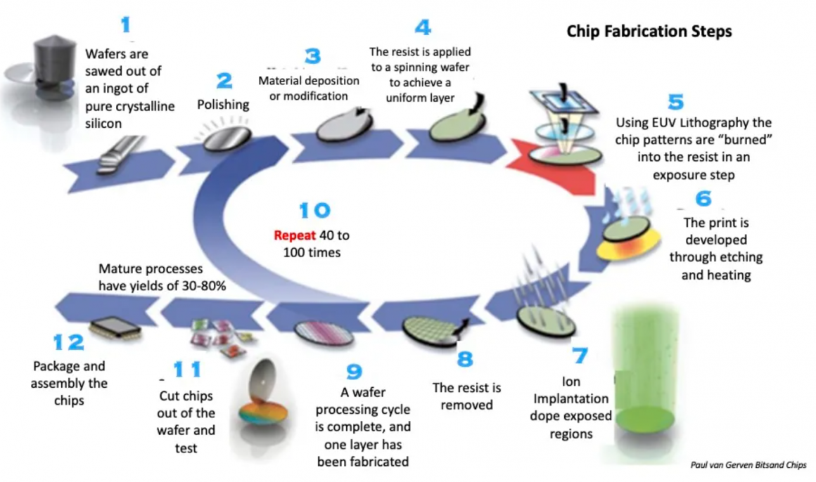
Value add distribution:
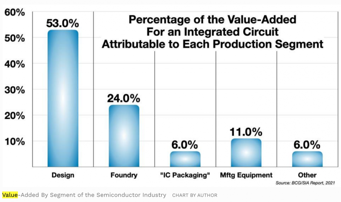
Like many other industrial products, semiconductors require (i) the design of chips, (ii) chip fabrication in the foundry, (iii) packaging of chips, (iv) manufacturing equipment, and others. Each contributes to value addition at different steps leading to final products. To understand the value addition of the semiconductor value chain, it’s good to have some knowledge about the relative contribution of each of these areas in the final value add. According to a study published by BCG and the Semiconductor Industry Association, in April 2021, the design adds the most value—as high as 43 percent of $600 billion revenue.
Semiconductor value chain as a pyramid:
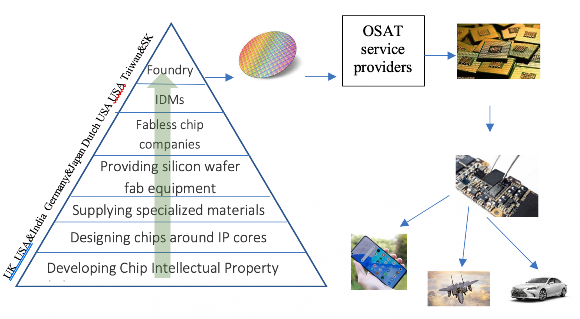
To comprehend this critical industry, let’s look into the value chain that involves peeling through several layers and repeating that process several times. If we vertically slice the industry, we find eight significant layers:
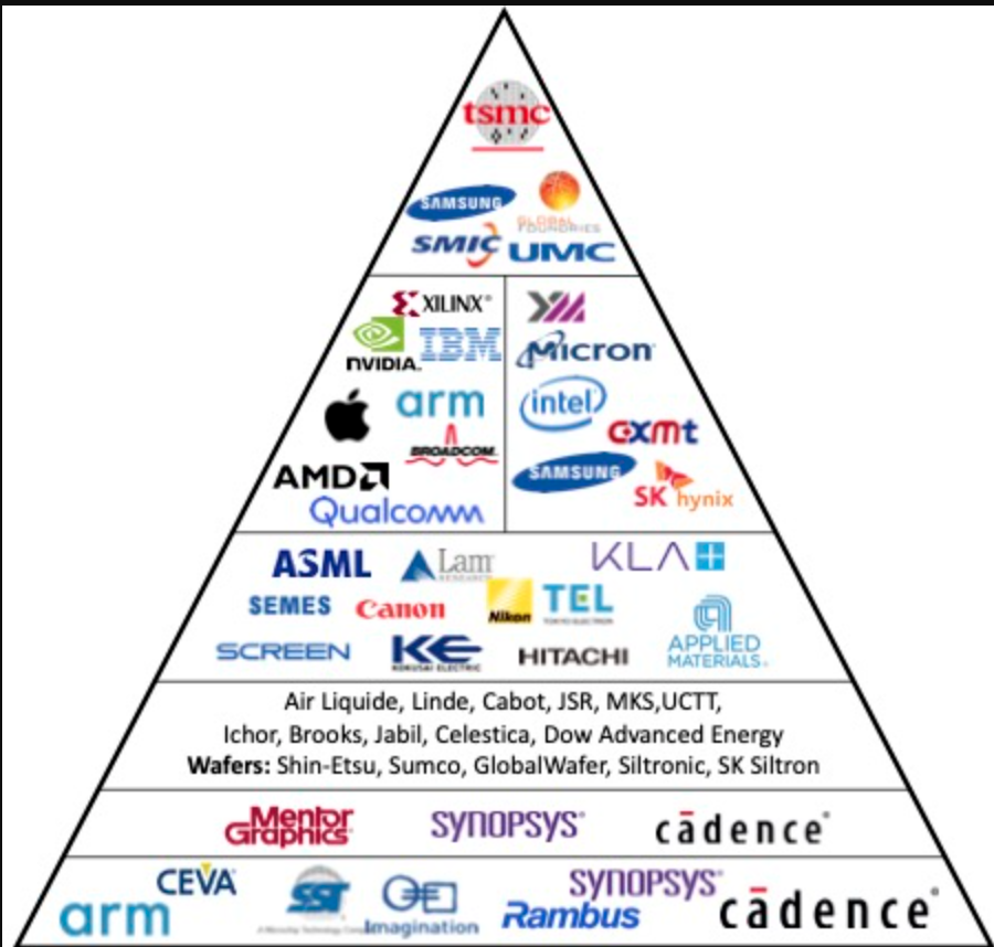
Source: Major firms in the semiconductor value chain-forming global ecosystem of semiconductor. Source: https://steveblank.com/
- Developing Chip Intellectual Property (IP) Cores—core ideas or building blocks forming the foundation of the chip
- Designing chips around IPs, using Electronic Design Automation (EDA) software tools, as layers of data
- Supplying specialized materials for fabricating or printing the design as layers of metals.
- Developing and providing silicon wafer fab equipment
- Designing, marketing, and selling chips–“Fabless chip companies.”
- Integrated device manufacturing (IDM)
- Chip making services from 3rd party foundries
- Chip testing and packaging services—delivered by Outsourced Semiconductor Assembly and Test (OSAT) companies
Major companies operating in each of the first seven layers of the value chain are shown in the adjacent figure. Each of these distinct industry segments feeds its resources up the value chain to the next. Hence, the output from the 3rd party chip factory (Foundry) depends on each lower layer to supply all the designs, equipment, and materials necessary to manufacture a chip.
Development of IP cores:
Every complex chip is not designed from scratch. Instead, designers use reusable building blocks of logic, cell, or IC layout design—like calling library functions in software development. These reusable blocks are semiconductor intellectual property cores (SIP core), IP cores, or IP blocks. They are intellectual properties, and owning companies license them. In the chip design, licensing of IP cores came into common practice in the 1990s. Chipmakers get a license of IP cores for reducing cost and shortening developing time. For example, Apple licenses IP Cores from ARM as a building block of their A-series processors for iPhones.
More than 150 companies that sell chip IP Cores generated USD 5.5 billion in 2021. The top five IP core licensing companies are ARM (41% market share in 2020), Synopsis, Cadence, SST, and Imagination Technologies. It’s expected that total revenue from IP core licensing will grow to USD 7.2 billion by 2026, at a cumulative average growth rate (CAGR) of 5.4%.
Chip designing using EDA tools:
With the help of EDA tools, engineers design chips by adding their designs on top of the required IP cores they’ve bought. For designing a complex logic chip like microprocessors powering smartphones, a large engineering team works for 2-3 years. Major steps in designing semiconductors are:
- System specification
- Architectural design
- Functional & Logic design
- Circuit design
- Physical design
- Physical verification
Those design steps lead to chip description as metal layout in GDSII, OASIS format. Due to the growing complexity of design, major EDA tool makers like Cadence, Mentor Graphics, and Synopsys have been using AI aids in automating design procedures. As high as 50 percent of chip design and EDA tools revenue belong to US firms. India has developed a large chip design service industry for the cost advantage. For example, in India, over 20,000 engineers designed over 2,000 chips in 2021. Indian firms provide mostly low-end chip design and verification services for third parties.
Supply of specialized materials and gases:
The result of the above two steps produces chips in software. To transfer them into physical chips, we need chip factories of “fabs”. Fabs are short for fabrication plants – chip-making factories. Both Integrated Device Manufacturers (IDMs) and Foundries both have fabs. The difference is that IDMs use their fabs only to make their chips, whereas Foundries use their “fabs” to make chips for others.
“Fabs” make chips through numerous steps with the help of specialized materials and chemicals:
- Silicon wafers—produced by slicing ‘ingots’ grown in crystal growing furnaces by melting silica sand; these wafers make the base for chips. It captures almost 3 percent of the semiconductor value chain. So far, Japan is the global leader with a 60 percent market share of wafers. High patent intensity is the entry barrier into this segment.
- Ultra-pure over 100 gases are used in ‘fabs’—including bulk (oxygen, nitrogen, etc.) and exotic/toxic gases (fluorine, nitrogen trifluoride, arsine, etc.
- Fluids like photoresists, top coats, and CMP slurries
- RF generators– critical surrounding components of the plasma chamber in wafer processing.
Some companies engaged in developing, producing, and supplying these specialized materials and gases are Tok, Dupont, Sumitomo, Merck, JSR, CMS, Fujifilm, Shin-Etsu, Sumico, etc.
Making chips using Wafer Fab Equipment (EFE):
- Physically manufacture of the chips requires very sophisticated equipment. The top five companies in making these machines are Applied Materials, KLA, LAM, Tokyo Electron, and ASML.
- The bulk of the $15 billion in constructing 5nm ‘fab’ goes to these companies. For example, a state-of-the-art photolithography machine of ASML (a Dutch company) may cost $150 million; of course, others are not as expensive as this one.
- For slicing an ingot of silicon and manipulating its atoms on and below its surface, fab equipment is some of Earth’s most complicated (and expensive) machines.
- For example, ASML’s $150 million extreme ultraviolet (EUV) lithography bus-sized machines contains100,000 parts and 2 kilometers of cabling. The company requires 40 freight containers, three cargo planes, and 20 trucks for shipping the components.
These machines are at the core of Keeping Moore’s Law alive.
Designing, using, marketing, and selling chips–“Fabless chip companies.”
- Systems companies create chip designs (using IP Cores and their own designs), but they do not have “fabs .”They send the designs to “foundries” that have “fabs” for manufacturing them.
- Some of them use the chips exclusively in their own devices, e.g., Apple, Google, Amazon ….
- Some system companies such as AMD, Nvidia, Qualcomm, and Broadcom sell the chips to everyone.
- As these system companies do not own ‘fab,’ they do not own Wafer Fab Equipment or use specialized materials or chemicals.
- Through licenses, they do use Chip IP and Electronic Design Software to design the chips
Qualcomm, Nvidia, Broadcom, MediaTek, AMD, and Apple are among the top fabless chip companies. Revenues of Qualcomm, Nvidia, and Broadcom in 2019-2020 were $19.4b, $17.74b, and $15.41b, respectively. Due to high wage differential, developing countries with growing engineering graduates may target this segment.
Integrated device manufacturing (IDMs):
- Integrated Device Manufacturers (IDMs) have vertically integrated value chain activities such as designing and manufacturing in their own fabs; they sell their own chips. Despite having fabs, they do not make chips for other fabless companies.
- Among the three categories of IDMs, Micron and SK Hynix are top performers in memory. Intel is at the top in logic, and TI and Analog Devices are dominant players in the analog segment.
- Although they have their own ‘fabs,’ they may also take service from 3rd party foundries. For example, Intel sources 7nm services from TSMC.
- In the past, IDMs have a strategic advantage. But over the years, it has eroded substantially due to growing fab capital expenditure and growth of the fabless segment. Hence, among others, Intel has been setting up new fabs for offering 3rd party foundry services.
Chip making services from 3rd party Foundries:
- Foundries offer chip-making services to others. Economies of Scale advantage are the underlying strength of this segment of the semiconductor value chain.
- They came into existence, in the 1980s, due to the growing need for chip-making services for fabless companies and the reluctance of IDMs to offer that service.
- In addition to sourcing fab equipment from 3rd parties, they also design unique processes for using the equipment to make the chips.
- Instead of being fab operators, they have been developing proprietary intellectual assets in advancing the precision, leading to decreasing size of transistors, reaching 5nm.
- Among the Foundries, TSMC is the top in logic, giving Samsung the 2nd spot
- There are foundries specializing in making chips for analog, power, rf, displays, secure military, etc.
- From a humble beginning in the 1980s, Foundry revenue crossed the $100 billion mark in 2021; TSMC’s more than 50% market share indicates monopoly, notably, in the high-end segment.
- Growing capital expenditure for fabs, reaching $20 billion for 3nm, has fueled the monopoly of this segment of the semiconductor ecosystem.
Chip testing and packaging services:
- After a long journey, wafers reach packaging and testing service delivery nodes of the globally distributed semiconductor value chain.
- Outsourced Semiconductor Assembly and Test (OSAT) companies package and test chips made by foundries and IDM
- Facilities in Malaysia and Taiwan, among others, provide these services.
- In the $30b markets, top OSAT companies are notable ASE, Amkor, and JCET. Due to the low entry barrier and labor cost advantage, less developed countries may target this segment. For example, Malaysia took advantage of it.
The semiconductor value chain is a globally distributed ecosystem:
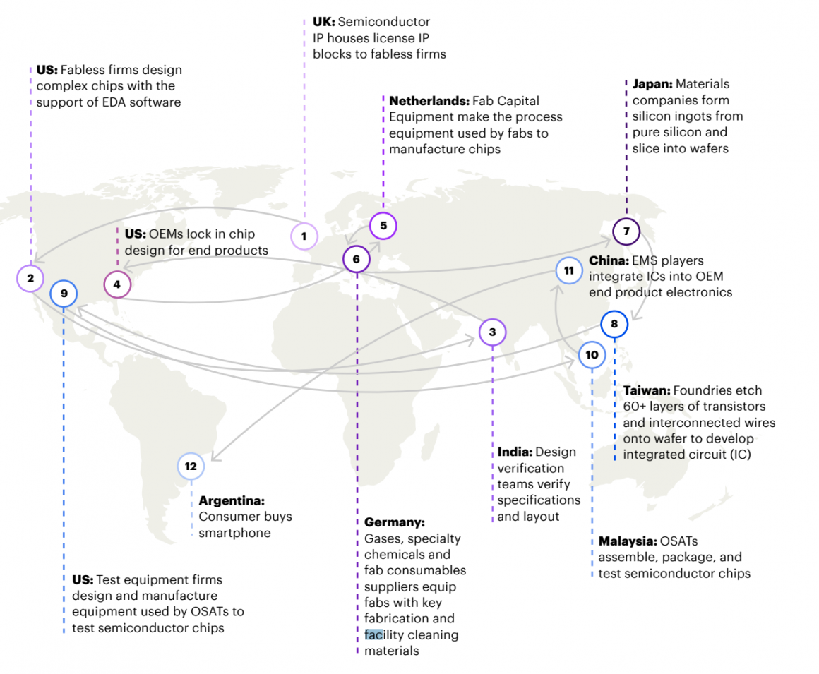
As explained, the collective semiconductor value chain enables semiconductors’ design, build, and delivery. However, this value chain is highly distributed across the globe. From the availability of science & engineering competence, prone to natural disasters, geopolitical risks, lead users to low-cost human resources, many factors have contributed to the spreading of this value chain, forming a global semiconductor ecosystem. Some of the central nodes in this ecosystem are below.
Central nodes of the semiconductor ecosystem:
- UK – Chip core IP firms like ARM develop and license IP blocks to fabless firms
- US – Fabless firms such as QUALCOMM and Apple design complex chips with the support of EDA software tools
- India – Due to wage differential, Indian engineers verify chip specifications and layout; they also offer other design services for low-end chips
- US – Original equipment makers(OEMs) like smartphones, computers, or automobiles, and system companies freeze chip design for end products
- Netherlands – Fab Capital Equipment makers like ASML offer high-end photolithography process equipment used by fabs to manufacture chips; firms from the USA, Japan, and others also provide fab equipment.
- Germany – Chemical companies supply ultra-pure gases and specialty chemicals; similarly, fab consumable suppliers equip fabs with critical fabrication and facility cleaning materials
- Japan – Materials companies form silicon ingots from pure silicon and slice them into wafers; for example, Japanese companies like Tokyo electrons supply fab equipment and fine chemicals
- Taiwan – Foundries such as TSMC etch 60+ layers of transistors and interconnected wires onto the wafer to develop integrated circuit (IC); Taiwan also have fabless, EMS, and OSAT companies
- US – Test equipment firms design and manufacture equipment used by OSATs to test semiconductor chips
- Malaysia – OSATs assembling, packaging, and testing semiconductor chips; IDMs like Intel also have plants for chip testing and packaging
- China – Electronics manufacturing service (EMS) players make PCBs, integrate ICs into OEM end product electronics; Foxconn-like companies assemble finished products.
- Across the world – Consumer buys a smartphone, computers, toys, and many more having printed circuit boards populated with chips or semiconductors.
Chips are becoming increasingly software machines:
Our common understanding about silicon chips has been that it’s about atomic-level manipulation of material properties for building skyscrapers in nano space. For example, memory chips are now made denser by stacking them 100+ layers high. Similarly, instead of making a single processor do all the work, logic chip designers have been stacking multiple specialized processors inside a chip. But enough change has taken place to make that perception incorrect. In addition to material, the software has been stacking up inside complex chips. For example, as high as 40 percent of the $500 million costs for 5nm complex chips is for on-chip software development. From 65nm to 5nm, this ratio has exponentially increased in favor of software.
Ever-evolving semiconductor value chain and ecosystem:
The semiconductor value chain comprises of highly synchronized functioning of linkages between thousands of suppliers from dozens of countries to add value at each step for turning the concept into a finished chip. Multiple factors have contributed to the distribution of this value chain as a global semiconductor ecosystem. Both the semiconductor value chain and ecosystem have still been transforming for improving the optimization and expanding scale and the scope of the industry. Upon taking advantage of discontinuity, new entrants like TSMC have become dominant players in these dynamics.
On the other hand, IDMs are disintegrating their value chains to become Foundries. Furthermore, due to the high scale effect of ideas and growing capital investment need, there has been a Natural tendency of monopoly. One of such effects has blunted the edge of a once highly successful vertical integration model, IDM. Hence, IDM role model Intel has been after entering the Foundry business. In retrospect, the underlying force of the evolution of the semiconductor value chain as a globally distributed ecosystem is the outcome of Schumpeter’s creative destruction. The semiconductor’s value chain and ecosystem evolution reflect the reality of industrial mutation that has been incessantly revolutionizing the economic structure from within, incessantly destroying the old one and continually creating a new one.
Foundries have economies of scale, standardization, and scope to utilize the entire stack of innovation in the ecosystem. Hence, once highly successful IDM model is weakening. But is Intel’s move to enter the foundry segment too late? Is it an indication that Intel and many other IDMs are desperate to withstand the creative destruction force of fabless firms and Foundries? Are we going to observe unfolding disruptive innovation examples in the semiconductor’s global chain? Will it have a significant transformation in the global semiconductor ecosystem?
...welcome to join us. We are on a mission to develop an enlightened community by sharing the insights of Wealth creation out of technology possibilities as reoccuring patters. If you like the article, you may encourage us by sharing it through social media to enlighten others.
Related Articles:
- Semiconductor Value Chain–globally distributed ecosystem
- Semiconductor Monopoly Due to Winning Race of Ideas
- Intel Falling Due to PC and Mobile Waves
- ASML Lithography Monopoly from Sustaining Innovation
- Taiwan’s Semiconductor Monopoly – How did it arise?
- ASML TSMC Nexus Fuels Semiconductor Monopoly
- ASML Monopoly in Semiconductor — where is magic?
Further questions:
By the way, I am wondering about a few pertinent questions:
1. Why did IDMs like Intel, TI, or Motorola overlook the opportunity of the Foundry model in the 1980s–giving the entry opportunity to TSMC?
2. Is Intel’s move to enter the Foundry business too late?
3. Does Intel’s move to foundry indicate disruptive innovation effect for IDMs is forthcoming?
4. What are the unfolding opportunities for new entrants?

